To additionally shrink electronic gadgets and to lower energy consumption, the semiconductor industry is keen on utilizing 2-D materials, however, producers need a fast and exact strategy for identifying defects in these materials to decide whether the material is appropriate for gadget manufacture. Presently a group of analysts has built up a method to rapidly and delicately describe defects in 2-D materials.
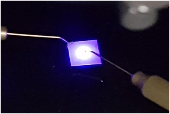
Two-dimensional materials are atomically thin, the most notable being graphene, a single-atom-thick layer of carbon atoms.
“People have struggled to make these 2-D materials without defects,” said Mauricio Terrones, Verne M. Willaman Professor of Physics, Penn State. “That’s the ultimate goal. We want to have a 2-D material on a four-inch wafer with at least an acceptable number of defects, but you want to evaluate it quickly.”
The analysts— who represent Penn State, Northeastern University, Rice University and Universidade Federal de Minas Gerais in Brazil—the solution is to utilize laser light joined with the second harmonic generation, a marvel where the frequency of the light shone on the material reflects at double the original frequency. They include dark-field imaging, a technique where superfluous light is sifted through with the goal that imperfections shine through. As indicated by the scientists, this is the first case in which dark-field imaging was utilized, and it gives three times the brightness of the standard bright field imaging strategy, making it conceivable to see kinds of imperfections already invisible.
“The localization and identification of defects with the commonly used bright field second harmonic generation are limited because of interference effects between different grains of 2-D materials,” said Leandro Mallard, a senior author on a recent paper in Nano Letters and a professor at Universidade Federal de Minas Gerais. “In this work, we have shown that by the use of dark field SHG we remove the interference effects and reveal the grain boundaries and edges of semiconducting 2-D materials. Such a novel technique has good spatial resolution and can image large area samples that could be used to monitor the quality of the material produced in industrial scales.”
Vincent H. Crespi, Distinguished Professor of Physics, Materials Science and Engineering, and Chemistry, Penn State, included, “Crystals are made of atoms, and so the defects within crystals—where atoms are misplaced—are also of atomic size.
“Usually, powerful, expensive and slow experimental probes that do microscopy using beams of electrons are needed to discern such fine details in a material,” said Crespi. “Here, we use a fast and accessible optical method that pulls out just the signal that originates from the defect itself to rapidly and reliably find out how 2-D materials are stitched together out of grains oriented in different ways.”
Another coauthor contrasted the method with finding a specific zero on a page loaded with zeroes.
“In the dark field, all the zeroes are made invisible so that only the defective zero stands out,” said Yuanxi Wang, an assistant research professor at Penn State’s Materials Research Institute.
The semiconductor industry wants to be able to check for defects on the production line, however, 2-D materials will probably be utilized in sensors before they are utilized in electronics, as per Terrones. Since 2-D materials are adaptable and can be consolidated into small spaces, they are good candidates for different sensors in a smartwatch or cell phone and the myriad of different places where small, adaptable sensors are required.
“The next step would be an improvement of the experimental setup to map zero dimension defects—atomic vacancies for instance—and also extend it to other 2-D materials that host different electronic and structural properties,” said lead author Bruno Carvalho, a former visiting scholar in Terrones’ group.
Disclaimer: The views, suggestions, and opinions expressed here are the sole responsibility of the experts. No Graph Daily journalist was involved in the writing and production of this article.